


The electronics manufacturing industry is evolving at a breakneck pace, driven by the relentless demand for smaller, faster, and more powerful devices. As consumer electronics, medical equipment, and industrial automation systems require higher computational power within shrinking form factors, traditional manufacturing methods often fall short. To meet these sophisticated demands, high-density interconnect technologies have become the gold standard. Among these advancements, bga pcb assembly stands out as a critical process for modern, high-performance electronics manufacturing, enabling dense component placement and superior thermal performance.
What is BGA PCB Assembly?
To understand why bga pcb assembly is so vital, it helps to understand what a Ball Grid Array (BGA) is. BGA is an advanced surface-mount technology (SMT) packaging method utilized for integrated circuits that require high-density connections. Unlike traditional surface-mount components that feature pins or leads extending from the perimeter of the chip, a BGA package utilizes the entire underside of the component. It features an array of miniature solder balls arranged in a grid across its bottom surface, which melt and bond directly with matching pads on the printed circuit board during reflow soldering.
Compared to conventional SMT, this approach significantly enhances pin density, allowing manufacturers to pack thousands of interconnections into a highly compact area. Furthermore, because the solder balls are positioned directly underneath the silicon die, the electrical path length is drastically reduced. This minimizes parasitic inductance and capacitance, leading to vastly improved overall electrical performance and signal integrity at high frequencies. Another major advantage is a reduction in thermal resistance; the direct physical connection allows heat to dissipate more efficiently away from the chip and into the PCB, preventing overheating in high-performance electronics.
Comprehensive Support for Diverse BGA Types
As a highly specialized process, assembling these components requires highly adaptable manufacturing lines capable of handling various substrate materials and pitch sizes. Modern applications call for a diverse range of BGA packages, each tailored to specific environmental and performance requirements:
- PBGA (Plastic Ball Grid Array): The most common cost-effective solution, utilizing a plastic substrate to provide reliable performance for general consumer electronics.
- CBGA (Ceramic Ball Grid Array): Engineered with a ceramic substrate, offering excellent thermal conductivity and robust reliability, making it ideal for high-end telecommunications and aerospace infrastructure.
- µBGA (Micro Ball Grid Array): Designed for extreme space-constrained environments like smartphones and wearables, featuring ultra-fine pitches.
- FCBGA (Flip-Chip Ball Grid Array): Connects the semiconductor die face-down directly to the substrate, shortening electrical paths and maximizing high-frequency performance.
- WLCSP (Wafer Level Chip Scale Package): Eliminates traditional packaging entirely by attaching solder bumps directly to the IC wafer, creating the smallest footprint possible.
- Stacked BGA Packages: Integrates multiple chips vertically within a single package to maximize memory and processing power in minimal space.
Strict Quality Control and Automated Inspection
Because the solder joints of a BGA component are hidden completely beneath the body of the chip, visual verification by human inspectors is impossible. Therefore, rigorous quality management practices must be implemented from raw material inspection through final product delivery to ensure the reliability and stability of every single solder joint.
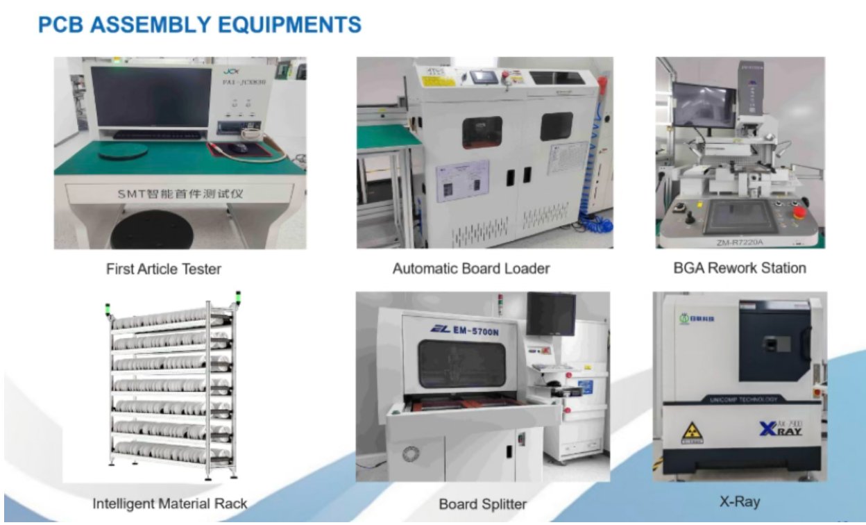
The primary line of defense in modern lines is Automated Optical Inspection (AOI). State-of-the-art AOI systems leverage high-precision visual recognition technology to scan the periphery of components swiftly, identifying placement deviations, missing components, or obvious solder defects before the board advances. This rapid and accurate detection enhances early-stage defect identification, significantly reducing rework costs. To complement AOI, high-density assemblies undergo advanced 3D X-ray inspection (AXI) to peer through the component bodies, ensuring there are no hidden voids, bridges, or weak interconnections underneath the chips.
Catering to Diverse Global Industries
The combination of dense integration and high reliability makes advanced assembly services invaluable across a spectrum of demanding global industries. In the medical field, devices such as advanced diagnostic scanners and patient monitoring systems rely on these dense interconnects to function safely and continuously. In industrial control sectors, automated assembly lines and heavy machinery electronics depend on robust solder joints to withstand harsh vibrations and thermal fluctuations.
Furthermore, telecom communication infrastructure, which manages massive amounts of data flow every second, requires the low-latency electrical paths provided by BGA configurations. Finally, semiconductor test boards utilize these capabilities to validate the next generation of microchips.
Your Trusted Partner for Quick-Turn Electronics
Navigating the complexities of advanced electronics manufacturing requires a partner with specialized infrastructure, engineering depth, and a commitment to speed. This is where FastTurn PCB excels. Established in 2015, we own a dedicated PCB factory and a state-of-the-art PCB assembly factory, employing approximately 350 skilled staff members. We focus entirely on providing comprehensive turnkey solutions for PCB fabrication and PCBA, excelling in small and medium-sized volume production while ensuring exceptionally quick delivery times.
With 70% of our high-reliability products proudly exported to Europe and America, and 30% serving other global markets, we understand international quality benchmarks and IPC compliance. When your project demands precision engineering, zero-defect reliability, and a rapid time-to-market, choose the agility and expertise of FastTurn PCB.
For more, visit Pure Magazine
